FAILURE ANALYSIS LEVEL 3
CROSS SECTIONING/OPTICAL MICROSCOPY
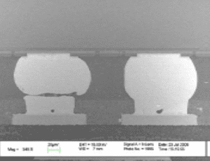
Innovative Circuits Engineering provides microscopic analysis that include cross sectioning, SEM and optical microscopy.
 Cross-sectioning combined with optical microscopy is a cornerstone technique in semiconductor failure analysis, providing direct visibility into the internal construction and physical condition of a device. By carefully cutting and polishing through the package or die, engineers can expose and examine critical layers and interfaces that are otherwise hidden. When viewed under an optical microscope, these cross-sections reveal valuable insights into material integrity, process quality, and potential failure mechanisms.
- Precise semi-automatic sample preparation of a wide range of materials for optical microscopy or SEM.
- Precision cross sectioning and parallel polishing in preparation for microscopic analysis (optical or SEM) of defects.
- Cross-sectioning is a failure analysis technique for mechanically exposing a plane of the area of interest in a die or package for further analysis or inspection.
- Parallel lapping is performed by lapping a silicon die down from the top, removing one metal layer at a time until the exact failure location is exposed.
- Backside die parallel polishing in preparation for backside emissions.