FAILURE ANALYSIS LEVEL 3
SEM/EDX TEST
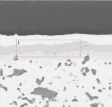 The purpose of SEM/EDX testing (Scanning Electron Microscopy with Energy-Dispersive X-ray Spectroscopy) is to analyze the surface structure and elemental composition of materials at high magnification and resolution. In the semiconductor industry, this powerful combination is widely used for failure analysis, quality control, contamination detection, and material characterization.
Common SEM/EDX Use Cases:
- Die and package failure analysis
- Cross-sectional analysis of solder joints or bond pads
- Material confirmation in process development
- Analysis of particles found during yield excursions